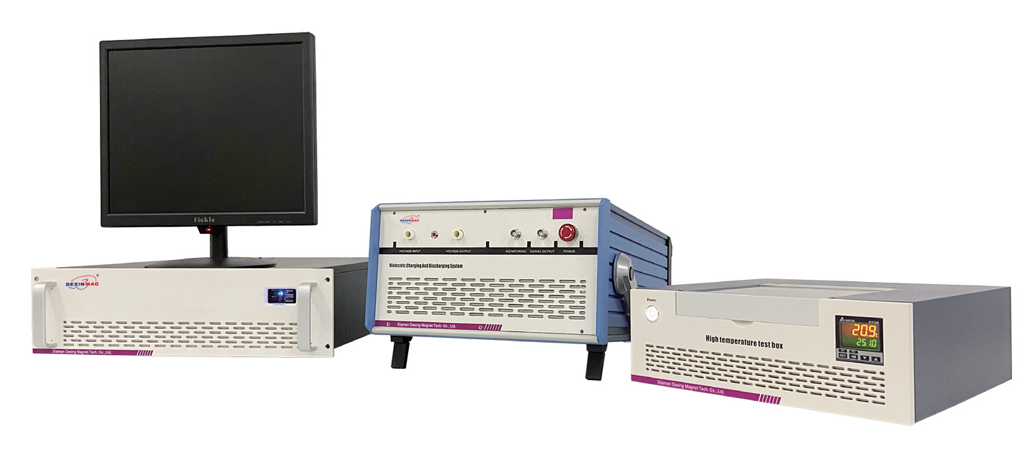
Dielectric Charging and Discharging System
Features
- Strong scalability: can be connected to an external high-voltage amplifier or high-voltage DC power supply;
- High discharge current: discharge current can be detected by current probe, up to 100A;
- Applicable to various sample tests: customized sample loading platform, suitable for ceramic and thin film sample testing;
- Data acquisition: collect data through oscilloscope, and can directly calculate energy storage density;
- Can be used as a signal source: can be used as a signal source to generate arbitrary waveforms;
- Variable temperature test: variable temperature test can be performed, RT~250℃;
- Polarized materials: can be used for polarized materials;
- Small parasitic capacitance and short action time: This system uses a special high-voltage switch to control the charging and discharging process through single-pole double-throw. The switch can withstand 10kV high voltage, small parasitic capacitance and short action time;
- Two test modes: realize under-damping and over-damping test modes. In under-damping test, the discharge circuit is short-circuited and no resistance load is used. In over-damping test, a larger precision non-inductive resistor is used as the discharge load;
- Fatigue test: fatigue test can be performed;
- Current and voltage: voltage 10kV, current 5mA.
Parameters
| Equipment model: | DX-DSC-10KV |
| Current probe bandwidth: | 120MHz |
| Peak current: | 0-100A, 150 A (multiple currents can be monitored) |
| Current acquisition accuracy: | 1mA |
| High voltage source module: | 3kV, 5kV, 10kV, 15kV are optional (current: 0-5mA) |
| Switch application: | 1 million times, withstand voltage 15kV |
| Temperature control range: | 0-200℃ |
| Temperature stability and accuracy: | 0.1℃ |
| Test samples: | thin film, thick film, ceramic, glass, etc. |
| Note: | Can be used with various polarization equipment to test various piezoelectric materials and dielectric materials |
Test Circuit
The DX-DCS-10KV energy storage dielectric charge and discharge system uses a specially designed capacitor discharge circuit for measurement. The test circuit is shown in the figure below.
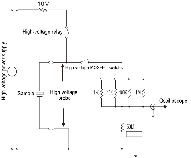
In this circuit, the dielectric film is first charged to a given voltage, and then the energy stored in the capacitor film is discharged to the resistor load by closing the high-speed MOS high-voltage switch. The time dependence of the voltage on the sample during the discharge process can be recorded by the detector. The energy storage performance of dielectric materials usually depends on the discharge speed, which can be adjusted by changing the resistance of the load resistor. Usually resistors with different resistances are installed in the test system. During the test, the user needs to select a resistor or a combination of several resistors to obtain the required resistance and connect the resistor or the combination of resistors to the dielectric material under test. In this circuit, it is very important to select a high-voltage MOSFET switch to release the stored energy. The switch limits the maximum discharge speed and maximum charging voltage of the circuit.
This test system consists of a discharge acquisition circuit, a high-voltage amplifier or a high-voltage DC power supply, and a control computer. During the test, the tester needs to determine the measured discharge speed by selecting a suitable resistor, and the voltage on the test sample can be automatically obtained by the computer.
Discharge Circuit
Similar to the P-E hysteresis measurement, prior to the discharge test, conductive electrodes should be prepared on the surface of the dielectric material and weak field dielectric properties that can be used to estimate the discharge rate of the test should be measured. Because high voltages of several kilovolts are often involved in the test, the dielectric material is usually immersed in silicone oil. The tester should determine the discharge rate they are interested in. The discharge rate can be roughly calculated from the low field capacitance C of the sample and the load resistance RL (RLC constant). Once the desired discharge rate is determined, the load resistor can be selected and connected to the test sample, and the charging voltage can be applied to the dielectric material. Once the sample is fully charged, the high speed switch is closed by pressing the discharge button on the circuit box, releasing the stored energy to the load resistor, and the time dependence of the voltage on the resistor can be automatically recorded by the computer.
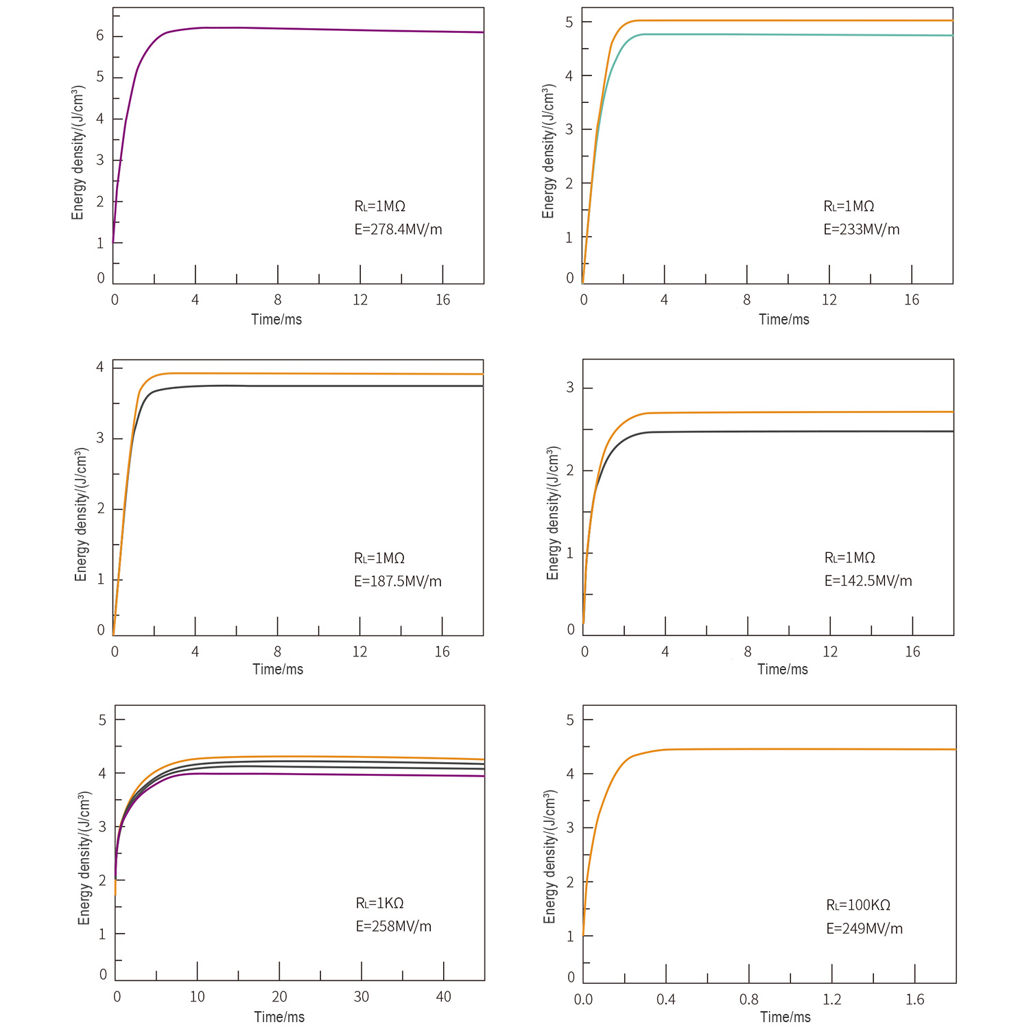
Here, P (VDF-TrFE-CFE) terpolymer (63/37/7.5) will be used as an example material to demonstrate how to interpret the discharge results. Using the circuit shown in the figure above, the discharge behavior of the terpolymer to the load resistor is characterized. Using the time-dependent voltage data formula, the time dependence of the discharge energy density can be calculated. The figure shows the discharge energy density of the terpolymer with a 1MΩ load for different charging electric fields over time. The total discharge energy density is comparable to the energy density derived from the unipolar P-E loop. The capacitance of the film sample used here was measured to be about 1nF at 1kHz. Characterization of several terpolymer film samples revealed that the discharge characteristics of the terpolymer cannot be simply described by the RC constant due to the nonlinear and frequency dependence of the polarization response, where R is the resistance (R=RL+ESR). Assuming that the capacitor capacitance does not vary with frequency, electric field, and the time constant of the RC circuit and the RC circuit (τ=RLC+ESRXC), if RL>ESR, ESRXC can be ignored, then the relationship between the discharge energy density and time is as follows: Uc(1)=UD(1-e-(21/t)) where UD is the discharge energy.
For ease of comparison, a 1nF capacitor and a 1MΩ load resistor are used to estimate the energy discharge time using the formula. The theoretical discharge time required for 70% energy release is 0.6ms, and the theoretical discharge time required for 50% energy release is 0.35ms. In the experiment, the discharge times required for these two energy releases were 0.66ms and 0.3ms, respectively. The difference between the estimated and measured values reflects the nonlinearity [the effective dielectric constant becomes smaller at high fields (>100MV/m)] and the frequency dependence of the dielectric response (the dielectric constant becomes smaller at higher frequencies or shorter discharge times). In addition, the ESR is small at high frequencies (or short discharge times) and the time after discharge becomes longer.
For the same terpolymer film capacitor, the discharge energy density under other load resistances (RLL is 100kΩ and 1kΩ, respectively) is shown in the figure. As expected, the reduced RL shortens the discharge time. However, a careful inspection of the experimental data shows that the reduction in discharge time is not proportional to the reduction in RL.