


Atomic Force Microscope
Features
1. Advanced functions: testing of physical quantities such as Young's modulus, adhesion, magnetic domain, surface potential, work function, etc.;
2. Adaptable environment: compatible with accessories such as culture dishes and heating tables, supporting underwater and high-temperature environment measurements;
3. Intelligent needle insertion: intelligent one-key needle insertion can be achieved with a piezoelectric scanning tube;
4. Adaptable size: 12-inch wafer and backward compatible with various wafer sizes.
Technical indicators
● Noise level in XY direction: 0.2 nm closed loop, 0.02 nm open loop;
● Noise level in Z direction: 0.06 nm closed loop, 0.03 nm open loop;
● Nonlinearity: 0.15% in XY direction, 1% in Z direction;
● Scanning mode: XYZ full probe scanning mode, the sample remains stationary during scanning;
● Scanning range: 90 μm×90 μm×9 μm;
● Scanning rate: 0.1 Hz~30 Hz;
● Image sampling points: 32×32~4000×4000;
● Sample size: 12-inch wafer is backward compatible with 8, 6, 4-inch and fragment samples;
● Working mode: contact, tapping, non-contact;
● Adaptive environment: air, liquid phase;
● Multifunctional measurement: electrostatic force microscope (EFM), scanning Kelvin microscope (KPFM), piezoelectric force microscope (PFM), conductive atomic force microscope (C-AFM), scanning capacitive force microscope (SCFM), magnetic force microscope (MFM), lateral force microscope (LFM), nano-etching/processing, single-point force spectrum curve, force modulation mode;
● Optional: fully automatic loading and unloading;
● Fully automatic probe approach system: 35 mm stroke, step accuracy 50 nm.
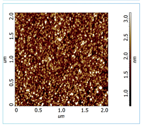
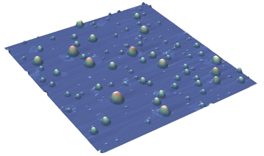
Tapping mode
Globular protein sample morphology image
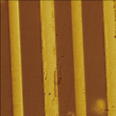
Actual case:

Au-Ti strip electrode potential
Scanning mode: KPFM (lift-off mode)
Scanning range: 18μm×18μm
Electrostatic force of Au-Ti strip electrode
Scanning mode: EFM (lifting mode)
Scanning range: 18μm×18μm
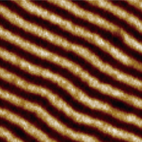
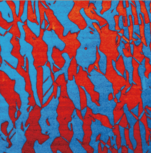
Fe-Ni thin film magnetic domain
Scanning mode: MFM (lift mode)
Scanning range: 14μm×14μm
PbTiO3-piezoelectric response vertical amplitude diagram
Scanning mode: PFM (contact mode)
Scanning range: 20μm×20μm
Polystyrene sphere morphology
Scanning mode: tapping mode
Scanning range: 10μm×10μm
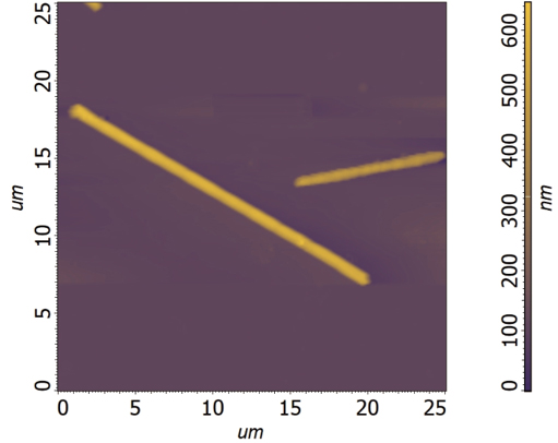
SiC whisker morphology
The electric sample positioning stage combined with optical imaging can achieve a positioning accuracy of 1 µm in a 300X300 mm area. The probe approach and scanning parameter adjustment are fully automated, and the imaging resolution can reach 20 picometers.